Physics and basic research
This generic term covers an extremely wide range of fields of research, from classical physics to modern quantum physics. JEOL solutions support the latest approaches to research – in particular with respect to questions regarding the investigation and analysis of substances of solid, liquid or gaseous consistency.
The resolution of the systems developed by JEOL extend into the atomic range and cover the entire periodic system.
Detailed solutions
- Analysing abrasive materials
Analysing abrasive materials
Abrasives contain particles of very hard, ceramic grains. Mechanically stripping the material structure to evaluate the corn and pore distribution is therefore very challenging. JEOL systems enable the simple, artifact-free production of large-scale cross-sections for examination.
Product groups
Solutions
Physics and basic research
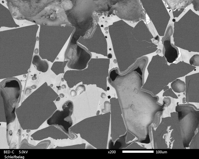 Cross-section through an abrasive material with boron nitride grains
Cross-section through an abrasive material with boron nitride grains
Source data: JEOL (Germany) GmbH, Diamant-Gesellschaft Tesch GmbH, data authorised for publication
- Analysing nanoparticles #2
Analysing nanoparticles #2
Due to their unique properties, nanoparticles are becoming increasingly important in industry as well as university research. Their chemical and physical properties depend heavily on their size, shape and composition. With the high-performance instruments from JEOL, these properties can be reliably analysed, even down to the sub-nanometer range.
Product groups
Solutions
Physics and basic research
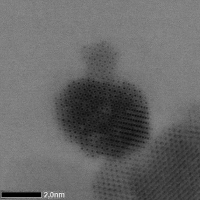 Electron microscope image of an iron oxide nanoparticle
Electron microscope image of an iron oxide nanoparticle
Source data: JEOL (Germany) GmbH, Bielefeld University, Dr. Ennen / Applied Research Paper F200
- Analysing nanoparticles
Analysing nanoparticles
Due to their unique properties, nanoparticles are becoming increasingly important in industry as well as university research. Their chemical and physical properties depend heavily on their size, shape and composition. With the high-performance instruments from JEOL, these properties can be reliably analysed, even down to the sub-nanometer range.
Product groups
Solutions
Physics and basic research
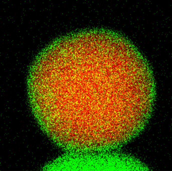 Element core-shell nanoparticle. The inner gold core (red) is covered by a 0.6 mm thin palladium layer (green).
Element core-shell nanoparticle. The inner gold core (red) is covered by a 0.6 mm thin palladium layer (green).
Source data: JEOL Ltd. / GrandARM presentation
- Characterising biofunctional surfaces
Characterising biofunctional surfaces
The surface of lotus leaves can serve as a model for self-cleaning surfaces. The exact characterisation of these surfaces is vital in order to be able to recreate them. The surface of lotus leaves comprises small wax tubes that can be easily destroyed during examination with an electron beam. JEOL therefore offers tailor-made solutions that thermally stabilise the samples in a controlled manner and thus prevent them from being destroyed by the observation.
Product groups
Solutions
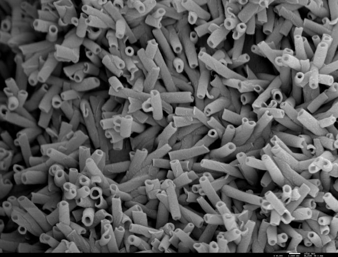 Surface of a lotus petal. The wax tubes have a diameter of approx. 50 nm
Surface of a lotus petal. The wax tubes have a diameter of approx. 50 nm
Source data: JEOL (Germany) GmbH
- Characterising lithium batteries
Characterising lithium batteries
Li batteries are used in mobile phones or vehicles, among other things. Thanks to the newly developed light element spectrometer from JEOL, detecting in a microscope has for the first time become routine and standard with high spatial resolution and detection sensitivity.
Product groups
Solutions
Physics and basic research
 Identification of lithium in an Li-ion battery
Identification of lithium in an Li-ion battery
Source data: JEOL Ltd., SXES brochure
- Characterising precipitates
Characterising precipitates
The formation of precipitates is used systematically to define the mechanical properties of a metallic structure. However, as a form of contamination, these can also be undesired. In order to be able to judge the quality of an alloy, it is necessary to determine the morphology and chemical composition of the precipitates. This is why JEOL supplies all-round, complete solutions, from artifact-free sample preparation to high-resolution analysis from the µm to the nm level.
Product groups
Solutions
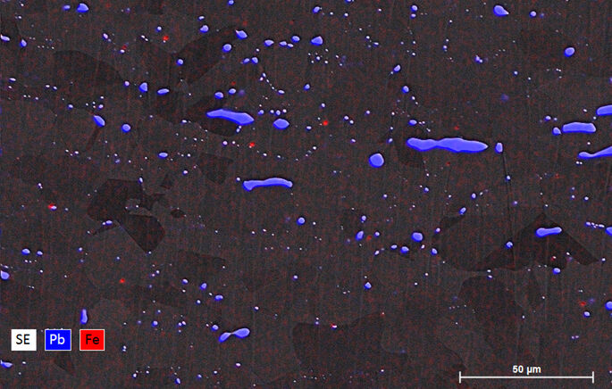 Element mapping image of a brass alloy
Element mapping image of a brass alloy
Source data: JEOL (Germany) GmbH
- Graphene analysis
Graphene analysis
The atomic imaging and analysis of light, electron-beam-sensitive materials requires high-performance microscopes. Thanks to their high stability and outstanding resolution, JEOL transmission electron microscopes are even capable of effortlessly identifying and examining lattice defects between individual carbon atoms.
Product groups
Solutions
Physics and basic research
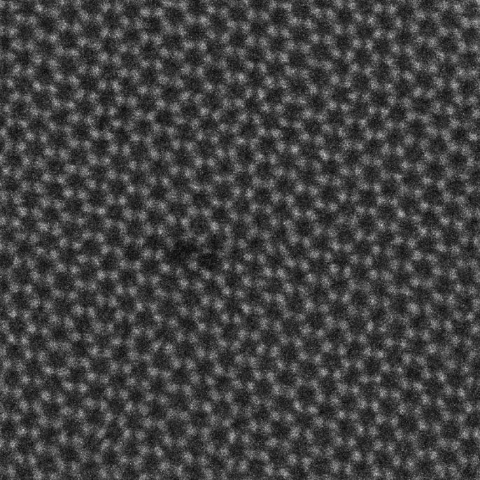 Atomic resolution image of graphene
Atomic resolution image of graphene
Source data: JEOL Ltd., GrandARM presentation
- High-resolution 3D reconstruction
High-resolution 3D reconstruction
High-resolution 3D images are essential for understanding the complex interrelationships of biological samples. With JEOL transmission electron microscopes it is possible to image sensitive biological structures without damaging them and reconstruct them by fully automated means in all three spatial dimensions. The calculated 3D model can be virtually moved, segmented and examined in any direction for a simple interpretation.
Product groups
Solutions
Physics and basic research
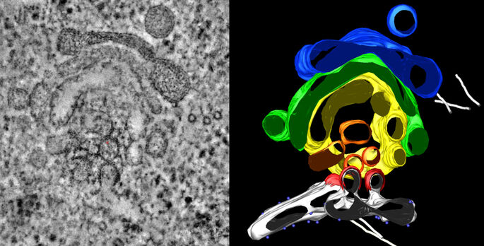 Electron microscope image and reconstructed model of a Golgi apparatus of a threadworm
Electron microscope image and reconstructed model of a Golgi apparatus of a threadworm
Source: JEOL (Germany) GmbH, ENI / Göttingen
- High-resolution bonding state analysis
High-resolution bonding state analysis
The properties of materials are essentially determined by their structure and the bonding states of the atoms. Precise knowledge of the structure and chemical composition are of key importance for the development of new materials. With the high-resolution spectroscopy systems from JEOL, it is possible to examine such bonding states locally with atomic precision.
Product groups
Solutions
Physics and basic research
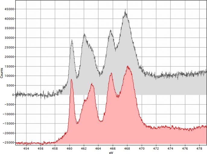 Energy loss spectrum of the minerals rutile (red) and anastase (grey)
Energy loss spectrum of the minerals rutile (red) and anastase (grey)
Source data: JEOL Ltd., ARM200F presentation
- In-situ presentation of microstructural changes
In-situ presentation of microstructural changes
During operation, materials are frequently exposed to high thermal loads, which change the microstructure or chemical composition of the material. In order to be able to examine this change in a scanning electron microscope, JEOL equips its EDX detectors with the option of recording the change over time. It is therefore possible to observe in-situ e.g. the grain growth and chemical separation caused by an external heat input.
Product groups
Solutions
Physics and basic research
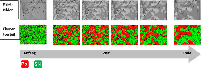 Thermally induced change to soldering tin (Pb Sn)
Thermally induced change to soldering tin (Pb Sn)
Source: JEOL Ltd.
- Light element analysis
Light element analysis
The combination of JEOL-patented TEM and EDX systems enables the detection of elements into the nm and sub-nm range. Modern techniques make it possible to achieve an accurate statement about the chemical composition within a very short time. This allows a time-efficient response to problems and questions.
Product groups
Solutions
Physics and basic research
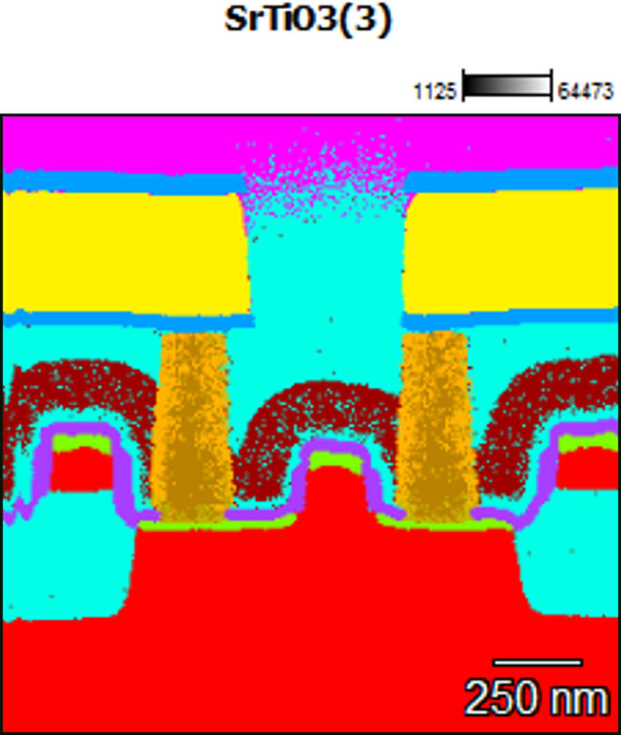 Chemical element mapping of a semiconductor sample (JEM-2800)
Chemical element mapping of a semiconductor sample (JEM-2800)
Source data: JEOL (Germany) GmbH, Demoreport AMS AG
- Microscale trace element analysis
Microscale trace element analysis
The detection of rare earths is not only of interest for mineralogical samples, it is also becoming increasingly significant due to the continuous development of high-performance microelectronics. For decades, JEOL has been setting the bar for detecting the mostly low-concentrated elements with its energetically and spatially high-resolution trace element analytics.
Product groups
Solutions
Physics and basic research
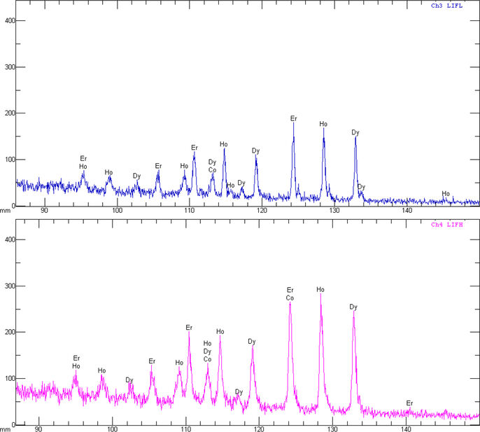 Rare earths as an example of trace element analysis
Rare earths as an example of trace element analysis
Source data: JEOL (Germany) GmbH, Demoreport Uni. Vienna (JXA)
- Mineral microstructures
Mineral microstructures
Minerals are frequently complex structures formed from a multitude of elements. Element mapping images are one of the most important methods for achieving the spatially resolved visualisation of the chemical composition. These mapping images can be used to gather essential information on e.g. the creation and structure of the samples under examination. For this task, JEOL supplies the most stable and most energetically and spatially high-resolution spectroscopy systems.
Product groups
Solutions
Physics and basic research
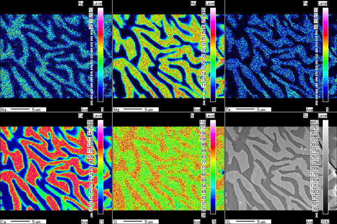 Element mapping images of a symplectite microsection
Element mapping images of a symplectite microsection
Source data: JEOL (Germany) GmbH, Demoreport Uni. Vienna (JXA)
- Semiconductor analysis
Semiconductor analysis
In modern semiconductor components, complex, functional structures have to be installed in an ever smaller space. In order to be able to reliably pinpoint and identify faults, it is essential to analyse precisely the structure and the element map. With the automated systems from JEOL, it is possible to prepare, image and analyse semiconductor components for faults precisely with the greatest accuracy.
Product groups
Solutions
Physics and basic research
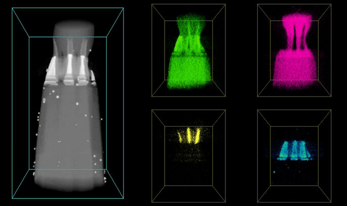 Three-dimensional element map of a NAND circuit
Three-dimensional element map of a NAND circuit
Source data: JEOL Ltd., JEM-2800 brochure/presentation
- Structur analysis of multi-layer systems
Structur analysis of multi-layer systems
For functionalised high-performance materials, the need for the controlled application of multi-layer systems on a substrate is becoming increasingly important. Specifically in the context of protective layers on metallic substrates, these systems make an important contribution to improving the longevity of heavily stressed components. In order to be able to image the chemical composition and the microstructural properties, JEOL has developed instruments that make it possible to prepare multi-layered components and map them to a previously unavailable depth of detail.
Product groups
Solutions
Physics and basic research
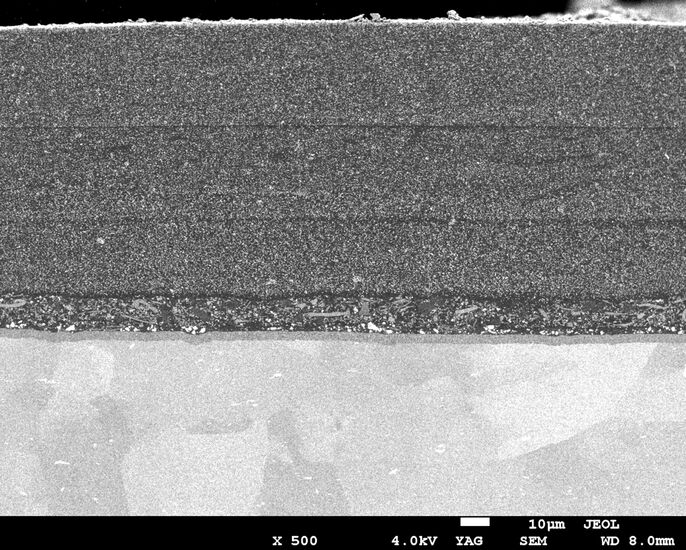 Layers of paint on an Al substrate
Layers of paint on an Al substrate
Source: JEOL (Germany) GmbH
- Structure / cross-section of electronic components
Structure / cross-section of electronic components
In the electronics industry, integrated circuits and components have to be connected by wires. The failure of this interface is one of the commonest causes of failure of these components. Characterising the quality of this interface requires pinpoint-accurate cross-sectional preparation without any thermomechanical load on the wire. JEOL systems enable the quick, simple, artifact-free and pinpoint-accurate preparation and detailed characterisation of this interface.
Product groups
Solutions
Physics and basic research
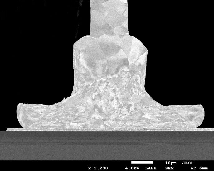 Cross-section through the bond pad of a light emitting diode.
Cross-section through the bond pad of a light emitting diode.
Source data: JEOL (Germany) GmbH
- Surface characterisation of functional materials
Surface characterisation of functional materials
More and more frequently, innovative materials are being tailor-made to their areas of application. Such precise modifications frequently occur even down to the nanoscale. Characterising such sensitive surfaces places the highest of demands on the imaging device. The high-resolution scanning electron microscopes from JEOL routinely operate within this threshold range.
Product groups
Solutions
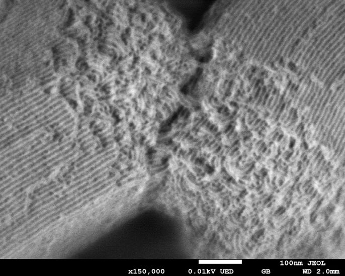 Surface image of a zeolite compound
Surface image of a zeolite compound
Source: JEOL Ltd.
- Texture and element mapping of metallic materials
Texture and element mapping of metallic materials
Modern metallic materials are frequently formed of complex systems comprising various constituents. The spatial orientation of the individual crystals (texture) and chemical composition are important components with respect to the resulting mechanical properties. In order to be able to detect both the texture and the chemical composition in parallel, JEOL supplies powerful complete solutions from artifact-free sample preparation to comprehensive three-dimensional reconstruction. This enables the direct comparison of both analytical techniques.
Product groups
Solutions
Physics and basic research
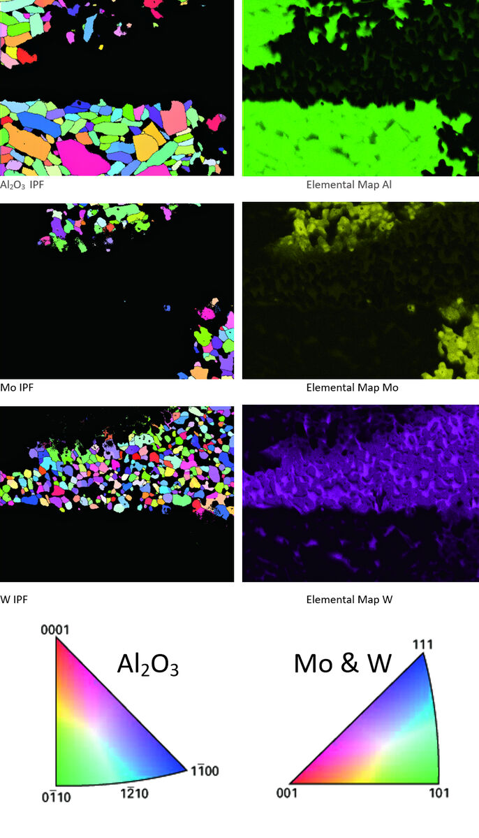 Mulit-layered circuit on a ceramic substrate (Al2O3, Mo, W)
Mulit-layered circuit on a ceramic substrate (Al2O3, Mo, W)
Source: JEOL Ltd.
- Writing and characterising semiconductor systems
Writing and characterising semiconductor systems
Photolithography is an essential method in semiconductor and microelectrical technology for manufacturing integrated circuits with high throughput. Electron-optical systems from JEOL enable fast, reliable quality assurance, as well as the optimisation and development of new processes in semiconductor technology.
Product groups
Solutions
Physics and basic research
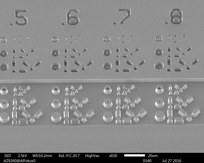 Photolithographically structured silicon wafer
Photolithographically structured silicon wafer
Source: JEOL (Germany) GmbH, Max-Planck-Institut für Halbleiterforschung, Munich.
